FM ADAPTOR

>> Thursday, April 15, 2010

Description.

With this compact FM adaptor circuit plugged into the audio out of your cassete player or i Pod out put,you can listen your favorite music on your car stereo.This circuit is very useful if your car stereo doesnot have an auxillary in socket.The circuit is nothing buy an short range FM transimitter.

The FM transmitter circuit is based on low power NPN transistor 2N2222.The tank circuit consisting of L1 & C1 producess the necessary oscillations at the collector of Q1.The capacitance C4 , resistance R3 & R4 performs the function of mixing the stereo out put from theaudio player or i-Pod.The emitter resistance R2 provides sufficient stability to the circuit.It also limits the collector current to increse the battery life.

Circuit diagram with Parts list.


Notes.

  • Use a 28SWG , 10 cm insulated copper wire as antenna.
  • For L1.make 8 turns of 20 SWG insulated copper wire on a 5mm dia plastic former.
  • Power the circuit from a 3V battery.
  • Assemble the circuit on a good quality PCB or common board.
  • C1 can be a 50pF trimmer.

Read more...

USB LAMP

>> Wednesday, April 14, 2010

>

Description.

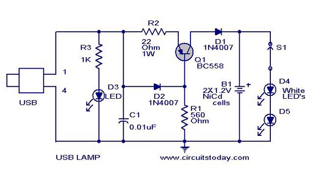
Here is a simple USB powered lamp that can be used to light your desktop during power failures. The circuit operates from the 5 V available from the USB port.The 5V from the USB port is passed through current limiting resistor R2 and transistor Q1. The base of transistor Q1 is grounded via R1 which provides a constant bias voltage for Q1 together with D2.The diode D1 prevents the reverse flow of current from battery.C1 is used as a noise filter.Two white LED’s are used here for the lamp, you can also use a 2 V torch bulb instead of LED’s. LED D3 indicates connection with USB port.

Circuit Diagram with Parts List.

Read more...

USB SOUND CARD

Description.
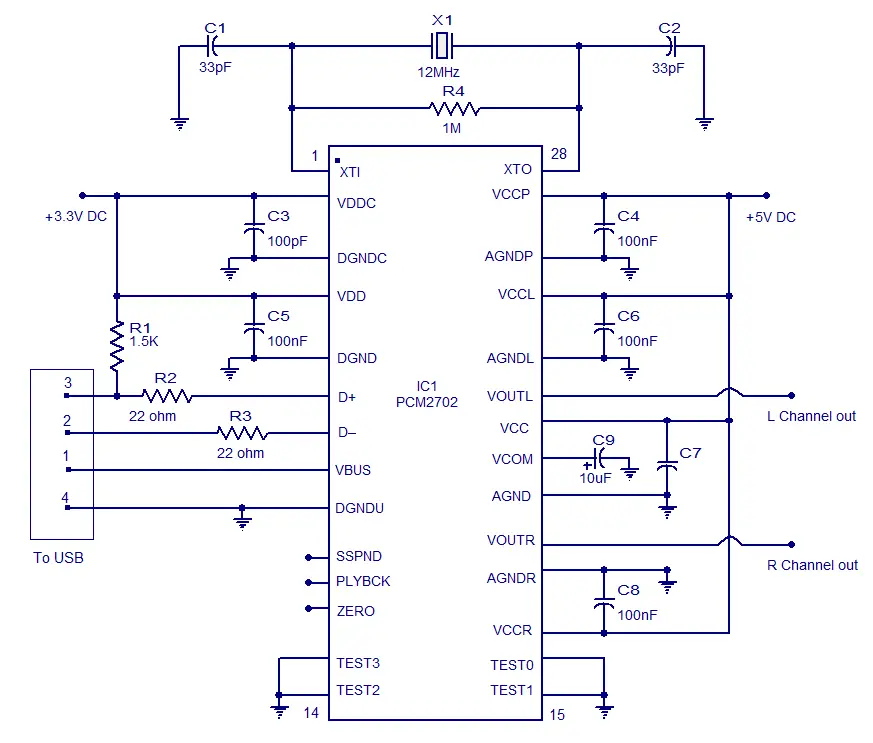
Designing and building a USB sound card is no longer a head ache because we have got the PCM 2702 integrated circuit from Texas Instruments. The PCM2702 is an integrated 16 bit digital to analog converter that has two digital to analog output channels. The integrated interface controller of PCM2702 is compliant to the USB 1.0 standards. The IC can handle sampling rates of 48 KHz, 44.1 KHz and 32 KHz. The IC also has a number of useful features like on-chip clock generator, digital attenuator, play back flag, suspend flag, zero flag, mute function etc. The most interesting thing is that this circuit is plug & play and doesn’t need any driver software for Windows XP and Windows Vista operating systems.

The circuit gets control data and audio data from the USB through the D+ and D- pins of the PCM2702 all the data transferring is carried out at full speed. The decoded audio signals will be available at the VOUTL and VOUTR pins of the IC. The 12MHz crystal is connected between the XT0 and XT1 pins of the IC. The VBUS (USB bus power) pin and DGND (digital ground) pins of the IC are connected to the +5V and ground pins of the USB respectively. The circuit requires +5V DC and +3.3V DC for operation and both of these voltages can be derived from the USB port using LDO (low drop out) voltage regulators (not shown in circuit).

Circuit diagram.

USB sound card

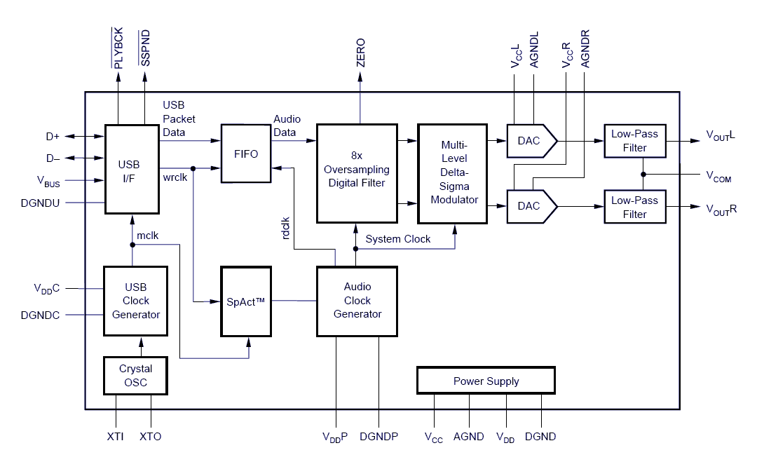
Block diagram of PCM2702.

PCM2702 block diagram

Notes.

  • +5V DC supply can be derived from the USB port using a +5V LDO regulator.
  • +3.3V DC supply can be derived from the USB port using a +3.3V LDO regulator.
  • Audio signals (output) available at VOUTL and VOUTR requires further amplification for driving low impedance head phones or loud speakers.
  • The PCM2702 is available only in SSOP28 package and requires special care while assembling.
  • Before attempting this circuit please go through the datasheet of PCM2702 and get a clear idea about the device.

Read more...

electronic keypad

Electronic Keypad electronic circuit diagram

Desctiption:

The IC is a quad 2 input "AND" gate, a CMOS 4081. These gates only produce a HIGH output, when BOTH the inputs are HIGH. When the key wired to 'E' is pressed, current through R1 and D1 switchs Q5 on.The relay energises; and Q5 is 'latched on' by R8. Thus, the Alarm is set by pressing a single key,say one of the two non-numeric symbols.

The alarm will switch off when the 4 keys connected to "A,B,C,D" are pushed in the right order.The circuit works because each gate 'Stands' upon its predecessor.If any key other than the correct key is pushed, then gate 1 is knocked out of the stack, and the code entry fails. Pin 1 is held high by R4. This 'Enables' gate 1; and when button 'A' is pressed, the output at pin 3 will go high. This output does two jobs.It locks itself 'ON' through R2 and it 'Enables' gate 2, by taking pin 5, high. Now, if 'B' is pressed, the output of gate 2, at pin 4 will go high. This output does two jobs. It locks itself 'ON' through R3 and it 'Enables' gate 3 by taking pin 12 high.

Now, if 'C' is pressed, the output of gate 3 will lock itself 'ON' through R5 and, by taking pin 8 high, 'Enable' gate 4. Pressing 'D' causes gate 4 to do the same thing; only this time its output, at pin 10, turns Q4 'ON'. This takes the base of Q5 to ground, switching it off and letting the relay drop out. This switches the alarm off.

Any keys not connected to 'A B C D E' are wired to the base of Q1. Whenever 'E' or one of these other keys is pressed, pin 1 is taken low and the circuit is reset. In addition, if 'C' or 'D' is pressed out of sequence, then Q2 or Q3 will take pin 1 low and the circuit will reset. Thus nothing happens until 'A' is pressed.Then if any key other than 'B' is pressed, the circuit will reset. Similarly, after 'B', if any key other than 'C' is pressed,the circuit will reset. The same reasoning also applies to 'D'. The Keypad needs to be the kind with a common terminal and a separate connection to each key. On a 12 key pad, look for 13 terminals. The matrix type with 7 terminals will NOT do. Wire the common to R1 and your chosen code to 'A B C D'. Wire 'E' to the key you want to use to switch the alarm on. All the rest go to the base of Q1.

The diagram should give you a rough guide to the layout of the components, if you are using a stripboard. The code you choose can include the non-numeric symbols.In fact, you do not have to use a numeric keypad at all,or you could make your own keypad. I haven't calculated the number of combinations of codes available, but it should be in excess of 10 000 with a 12 key pad; and, after all, any potential intruder will be ignorant of the circuit's limitations. Of Course, if you must have a more secure code, I can think of no reason why you shouldn't add another 4081 and continue the process of enabling subsequent gates. Or you could simply use a bigger keypad with more "WRONG" keys. Any small audio transistors should do. The 27k resistors could be replaced with values up to 100k. And the only requirements for the 4k7 resistors is that they protect the junctions while providing enough current to turn the transistors fully on. Capacitors (C1 C2 C3 C4 C5) are there to slow response time and overcome any contact bounce. They are probably unnecessary.

Read more...

single chip fm radio

Description.

Here is a compact low cost FM radio circuit using IC7400. This circuit is designed as per the data sheet and the result is excellent.Ideal for all category of electronic enthusiasts.

The TDA7000 is a monolithic integrated circuit for mono FM portable radios, where a minimum on peripheral components is crucial. The IC TDA 7000 has a Frequency-Locked-Loop system with an intermediate frequency of 70 kHz. The intermediate frequency selectivity is achieved by active RC filters. The only function which needs alignment is the resonant circuit for the oscillator, thus selecting the reception frequency. Spurious reception is avoided by means of a mute circuit, which also eliminates too noisy input signals. Special steps are taken to meet the radiation requirements.

Circuit Diagram with Parts List.


Notes

  • For L1 and L2 wind 5 turns of 0.6 mm enameled Copper wire on a 4 mm dia plastic former.
  • For antenna use a 50mm long insulated copper wire.
  • IC TDA 7000 can withstand up to 10 V supply voltage.But I recommend 6V.
  • Use an 8 Ohm speaker or Headphone at the audio output.

Read more...

ONE TRANSISTOR FM RECEIVER


This radio

is sensitive enough to tune 20 stations across the FM band, some with volume high enough to drive a small PM speaker. The ability to tune 88.9 MHz and 89.1 MHz is testimony of its selectivity. The signal-to noise ratio rivals that of the better walkman type radios.

Read more...

LONG DISTANCE VIDEO WIRE

This circuit is used to connect the camera with very log wire. This is actually a video amplifiers. This circuit consist of two part, they are sender part and receiver part. At the sender part, this circuit uses an amplifier to make a stronger signal. So the signal can be transmitted through the long cables. To transmitted the signal, this circuit uses balanced mode, where two wires are driven in the opposite phase. Here is the schematic diagram :

video wire circuit circuit schematic diagram
The resistance of a typical four conductor flat 28 gauge telephone wire is about 7 ohms per 100 feet. Since voltage drops appear in both the plus and minus power supply leads, the total series resistance is about 14 ohms per 100 feet. Maximum allowable wire length depends on the total current requirements of the camera and send board. Using a camera that draws 100 ma, for example, a total current of about 180 ma is required and therefore a maximum of approximately 500 feet of 28 gauge flat telephone wire can be used. If a longer wire is needed, the round type of 22 gauge four conductor telephone wire offers much lower resistance. Its resistance per 100 feet is approximately 3.3 ohms total for both the positive and negative power wires. Using this wire and a 100 ma camera, the wire length can be approximately 2000 feet.

Parts:
* C1 – 22 mfd 6.3 volt tantalum
* C2, C3, C4, C9, C10, C11, C12 – 1 mfd 16 volt tantalum
* C5 – 3.3 mfd 16 volt tantalum
* C6, C7 – 22 mfd 16 volt tantalum
* C8 – .1 mfd 50 volt metalized film
* C13 – 2200 mfd 50 volt electrolytic
* C14 – 1 mfd 50 volt tantalum
* R1, R15 – 75 ohms 1/8 watt
* R2, R9, R10 – 10K 1/8 watt
* R3 – 200 ohms 1/8 watt
* R4, R14 – 4.7K 1/8 watt
* R5, R6 – 51 ohms 1/8 watt
* R7 – 330 ohms 1/8 watt
* R8, R11, R13 – 100 ohms 1/8 watt
* R12 – 200 ohms potentiometer
* R16 – 160 ohms 1/4 watt
* R17 – 100K 1/8 watt
* R18 – 10K potentiometer
* R19 – 15K 1/8 watt
* R20 – 8.2 ohm 1/2 watt
* R21 – 150 ohm 1/8 watt
* R22 – 100 ohm potentiometer
* R dummy – 100 ohm 2 watt
* D1 – 12 volt 1 watt zener diode
* D2 – Motorola MVAM109 tuning diode
* D3 – 10 volt 1 watt zener diode
* BR1 – 1 amp 400 volt DIP bridge rectifier
* IC1 – Maxim MAX435 dual output amplifier
* IC2, IC3, IC5, IC6 – 78L05 voltage regulator
* IC4 – Maxim MAX436 single output amplifier
* IC7 – LM317 adjustable voltage regulator
* J1 – RJ11 6P4C telephone jack with leads
* J2 – RJ11 6P4C board mount telephone jack
* J3 – chassis mount angle coaxial F connector
* T1 – 24 volt AC 400 ma adapter transformer
* eight 6-32 X 1/4 inch screws
* rubber grommet for 1/4 inch hole
* 2.2 X 3.3 X 4 inch metal enclosure with vent holes
* four conductor telephone wire with RJ11 plugs
* TO220 5 watt clip on heat sink
* four threaded spacers 6-32 X 1/2 inch long

The MAX435 transconductance amplifier is used as the core of this circuit. This circuit has wide bandwidth feature that is suitable for video signal application. To make sure that any noise exposing the cables would cancel each other at the receiver, this circuit uses balanced mode.

Read more...

water level controller

A controller for keeping the water level stays between upper and lower limits is described here. This water level controller is actually a water pump controller that turn the pump on or off based on the detected water level. This water level controller has two modes: fill and empty. Here is the schematic diagram of the circuit:

water pump controller circuit schematic diagram

For the empty mode, the water pump is used to suck the water from the tank. If the water reach the upper level limit, the pump will be turned on to drain the tank, until the level falls down to the lower level limit. At the fill mode, the pump is used to fill the tank with water, thus if the water level falls below the lower limit, then the pump will be turned on to fill the tank with the water. The SW1 set the mode, with the empty mode default value (as shown in the schematic).


Read more...

sound operated relay

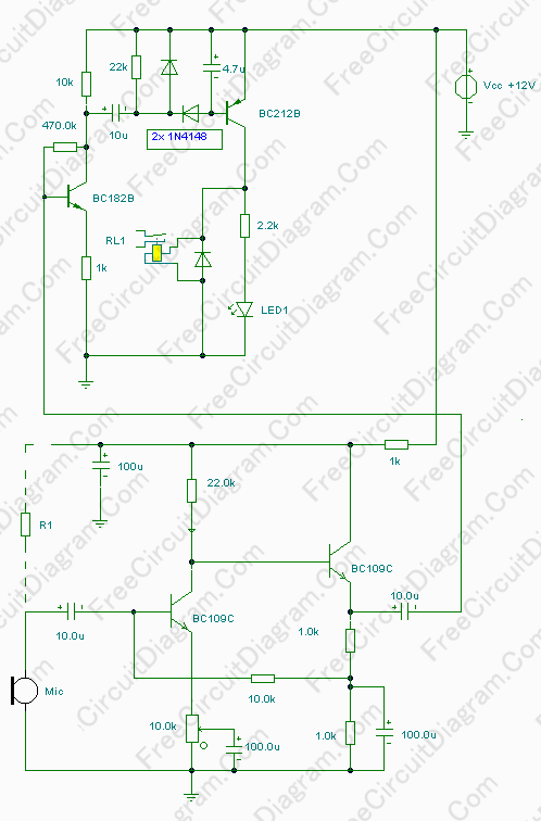
This circuit is not a voice operated switch (VOX) because this circuit is too dumb to differentiate between musical sound or human voice. This is rather a sound activated than voice activated. One interesting application is to control your disco lighting automatically by the musical sound from high power amplifier, when the music signal is dominating the sound space. The schematic diagram is shown below.

voice operated switch circuit schematic

You can use either moving coil microphone or condenser microphone for this circuit. For condenser microphone, you have to connect R1 resistor as shown by the dashed line. Choose between 1k5 ad 22k to adjust the sensitivity, or use a 4k7 value if you don’t care with the sensitivity fine tuning. Make sure the electrolytic capacitor is rated for 16 volt or more. The potentiometer shown in the schematic diagram is used to adjust the gain of the pre-amplification. You can adjust this potentiometer to get a proper sound level where the relay would be activated

Read more...

SIMPLE TEMPERATURE CONTROLLER

DESCRIPTION:
This temperature controller employs an LM135/235/335 temperature sensor, can be used to keep small environment warm or hot. Here is the schematic diagram:

Simple temperature controller

LM311 is used as comparator, to detect if the voltage at sensor pin (the inverting input) goes higher than the reference pin (the non-inverting pin). If this condition is detected, the comparator will switch off the heater driver (BUV26). Practically, after the desired temperature is met, the heater will be oscillating on-off, trying to keep the voltages at non-inverting input and inverting input equal

Read more...

positive to negative power supply by using simple 555 ic

DESCRIPTION:

If you need a negative supply for op-amp or just need negative bias voltage while operating from a single supply voltage (for battery operation for example), this circuit helps providing the negative supply for you. The circuit is based on charge pump driven by 555 switching circuit. Here is the schematic diagram:

negative supply 555 circuit schematic


The negative voltage produced by this circuit is about 1 volt smaller than the positive supply voltage magnitude. If you use 9V positive supply then the negative output will be around 8 volt, or if you use 12 volt positive supply the you’ll get around 11Volt negative supply. 100mA current could be drawn safely from the negative voltage output. This is enough for most op-amp or other small signal application.

Read more...

single tansistor FM

winding L1

L1 sets the frequency of the radio, acts as the antenna, and is the primary adjustment for super-regeneration. Although it has many important jobs, it is easy to construct. Get any cylindrical object that is just under 1/2 inch (13 mm) in diameter. I used a thick pencil from my son's grade school class, but a magic marker or large drill bit work just fine. #20 bare solid wire works the best, but any wire that holds its shape will do. Wind 6 turns tightly, side-by-side, on the cylinder, then slip the wire off. Spread the windings apart from each other so the whole coil is just under an inch (2.5 cm) long. Find the midpoint and solder a small wire for C2 there. Mount the ends of the wire on your circuit board keeping some clearance between the coil and the circuit board

Read more...

xmerless power supply

>> Tuesday, April 13, 2010

Description:

Here is a low cost and simple circuit that can be used to power up small electronics devices. The power is directly tapped from the mains via resistor R1.D1 rectifies the voltage and C1 and C2 are used to filter the output.The zener diode D2 keeps the voltage at steady 5V.


  • This circuit can deliver only up to 2omA ,there fore not suitable for serious circuits.
  • You can use this power supply for small LED circuits etc .
  • Remember you are playing with mains.Always be careful

Read more...

About This Blog

Lorem Ipsum

DISCLAIMER

I have not uploaded any contents on my own. I have got all these resources from the internet which are public and obtained as such from search engines. If these contents are objectionable or violating anyone copyrights please contact me. I will do the needful immediately and assure full assistance. No files are hosted on my server; they are only indexed much like how Google works. The hosting server or the administrator cannot be held responsible for the contents of any linked sites or any link contained in a linked site, or changes / updates to such sites. All stuff on this blog is for Entertainment and private Purposes only. It is not the purpose of this blog to infringe on anybody’s copyrights. Mail @ srikanth.tadhiparthi@gmail.com

  © Sunset by VINOD KUMAR 2008

Back to TOP