HI-FI DX BASS CIRCUIT

>> Friday, April 30, 2010

Description.

Here is the circuit diagram of a passive DX bass circuit that can be used with almost all audio amplifiers.

comments on the circuit : The circuit that I have designed is a passive one but you can make it an active one by adding a pre amp at the output. The first stage acts as a main tone stage. It balances the bass and the treble. The 0.01 cap is for high frequency while the 0.22uF cap is for low frequency. The second stage is for sound compression. the caps works the same as at the first stage only that they are there to start the sound compression that is received from the input stage. The 2.2k resistor delays the sound thereby multiplying the compression. The 10k variable resistor is there used to tune the compression depending on the frequency of the speaker. If you are using 4 to 6 inches hi-fi speakers, I advise you to keep the 10k variable resistor at 0 ohm. The circuit is not copyrighted and you can change it to suit your requirement. All I ask is to be posting the updates of the circuit design on the site.

Circuit diagram.


Circuit diagram.

Notes.

  • Assemble the circuit on a good quality PCB.
  • This circuit does not require a power supply.
  • POT R6 is for volume control.
  • Switch S1 can be a slide switch and it is the DX Bass switch.

Read more...

FM PHONE TRANSMITTER

>> Friday, April 23, 2010

This project provides the schematic and the parts list needed to construct a FM Phone Transmitter. This device attaches in series to one of your phone lines. When there is a signal on the line (that is, when you pick up the handset) the circuit will transmit the conversation a short distance. In particular it will radiate from the phone line itself. It is a passive device - there is no battery. It uses the signal on the phone line for power. No aerial is needed - it feeds back the RF signal into the phone line which radiates it in the FM band. The frequency of transmission may be adjusted by the trimcap. Note that some countries may ban any electronic device which attaches to the telephone. It is the responsibility of the constructor to check the legal requirements for the operation of this FM Phone Transmitter and to obey them.

FM Phone Transmitter Schematic


FM Phone Transmitter Circuit Description

The circuit is a radio frequency (RF) oscillator that operates around 93 MHz (93 million cycles per second). Power for the circuit is derived from the full wave diode bridge. C1, C8, L3 & T1 forms the FM oscillator.

Every Tx needs an oscillator to generate the Radio Frequency (RF) carrier waves. L1, C6, T2 forms the power amplifier. Audio from the telephone

lines is coupled through R3 & C2 into the base of T1 to modulate the oscillator. This is done by varying the junction capacitance of the transistor. Junction capacitance is a function of the potential difference applied to the base of the transistor. R1 & C4 act as a low pass filter.

C3 is a high frequency shunt. L2 is call a RFC (radio frequency shunt.) It decouples the power and audio from the transmitter amplifier circuit. This type of circuit usually should be calibrated. The resonant frequency of the L1-C6 amplifier circuit should be adjusted to match the resonent oscillator frequency of C1, C9-L3. However, in practice, we think you will find that the unit operates perfectly OK as it is constructed without the need to calibrate anything. If you want to try calibration you will need a frequency meter, a CRO or just trial and error.

Calibrate by moving the coils of L1 further apart. With C1 at 27p you will find that the it tunes into the FM band in the 86 - 95 MHz area. With C1 at 22p the band is raised to about 90-95mhz (depending in the coil spacing.) If you want to move this tunable area still higher to over 100MHz range then replace C1 by a 15pF or 10pF capacitor. This assumes that the on-hook voltage is about the standard 48V. If the on-hook voltage of an extension phone network is lower, say about 39V, C1 will have to be lower in the 15p to 10p range to be in the commercial FM band in this case.

Note that you should not hold the printed circuit board physically in your hands if you try to do any calibration. Your own body capicitance when you touch it is more than enough to change the oscillation frequency of the whole unit.

You can experiment the FM Phone Transmitter to get greater transmission range away from the phone line by adding an aerial (about 150 cm of 26 gauge wire) to the collector of T2.


FM Phone Transmitter Assembly Instructions

The ZTX320 has a flat and a curved side. Match these two sides with the flat and curved sides as shown on the overlay for T2. Also note these points when assembling this project:

1) Two of the three coils have enamel insulation lacquer on them. This must be physically removed from both ends of the coil before it can be soldered. Now during the manufacture of these coils they have been solder dipped to remove this lacquer. But check each leg to see that this is the case.

2) Spread out the turns in the L3 coil about 1 mm apart. The coils should not touch.

3) A solder connection (or tap) is required from the top of the first turn in the L3 coil to the pad next to the coil. Solder a piece of wire to the top of the first turn as shown on the overlay. Then solder the other end to the pad immediately next to the L3 coil.

4) The cathodes of all diodes point to the top of the PCB.

5) Attach 3" of wire with an alligator clip on the end to the pads between the diodes marked - 'TO LINE' No aerial is needed. The phone line itself acts as a sufficient aerial. To make the Kit small, resistors & diodes stand on their ends. The kit attaches to ONE of the two phone lines going to your phone. Either of the two lines will do. In most of the world this is the green or red wire. In the UK it is one of the wires attached to the terminals 2 or 5. Cut the phone line. Attach one alligator clip to one cut end and the other alligator clip to the other cut end. Take your phone off the hook and turn on an FM radio at about 93 MHz. It should be very easy to tune into the transmission. Take a portable FM receiver outside and follow the phone line.


FM Phone Transmitter Parts List


Read more...

3V FM TRANSMITTER

This project provides the schematic and the parts list needed to construct a 3V FM Transmitter

. This FM transmitter is about the simplest and most basic transmitter to build and have a useful transmitting range. It is surprisingly powerful despite its small component count and 3V operating voltage. It will easily penetrate over three floors of an apartment building and go over 300 meters in the open air.

It may be tuned anywhere in the FM band. Or it may be tuned outside the commercial M band for greater privacy. (Of course this means you must modify your FM radio to be able to receive the transmission or have a broad-band FM receiver.) The output power of this FM transmitter is below the legal limits of many countries (eg, USA and Australia). However, some countries may ban ALL wireless transmissions without a licence. It is the responsibility of the constructor to check the legal requirements for the operation of this kit and to obey them.


The circuit is basically a radio frequency (RF) oscillator that operates around 100 MHz. Audio picked up and amplified by the electret microphone

is fed into the audio amplifier stage built around the first transistor. Output from the collector is fed into the base of the second transistor where it modulates the resonant frequency of the tank circuit (the 5 turn coil and the trimcap) by varying the junction capacitance of the transistor. Junction capacitance is a function of the potential difference applied to the base of the transistor. The tank circuit is connected in a Colpitts oscillator circuit.


The electret microphone: an electret is a permanently charged dielectric. It is made by heating a ceramic material, placing it in a magnetic field then allowing it to cool while still in the magnetic field. It is the electrostatic equivalent of a permanent magnet. In the electret microphone a slice of this material is used as part of the dielectric of a capacitor in which the diaphram of the microphone formsone plate. Sound pressure moves one of its plates. The movement of the plate changes the capacitance. The electret capacitor is connected to an FET amplifier. These microphones are small, have excellent sensitivity, a wide frequency response and a very low cost.

First amplification stage: this is a standard self-biasing common emitter amplifier. The 22nF capacitor isolates the microphone from the base voltage of the transistor and only allows alternating current (AC) signals to pass.

The tank (LC) circuit: every FM transmitter needs an oscillator to generate the radio Frequency (RF) carrier waves. The tank (LC) circuit, the BC547 and the feedback 5pF capacitor are the oscillator in the Cadre. An input signal is not needed to sustain the oscillation. The feedback signal makes the base-emitter current of the transistor vary at the resonant frequency. This causes the emitter-collector current to vary at the same frequency. This signal fed to the aerial and radiated as radio waves. The 27pF coupling capacitor on the aerial is to minimise the effect of the aerial capacitance on the LC circuit. The name 'tank' circuit comes from the ability of the LC circuit to store energy for oscillations. In a pure LC circuit (one with no resistance) energy cannot be lost. (In an AC network only the resistive elements will dissipate electrical energy. The purely reactive elements, the C and the L simply store energy to be returned to the system later.) Note that the tank circuit does not oscillate just by having a DC potential put across it. Positive feedback must be provided. (Look up Hartley and Colpitts oscillators in a reference book for more details.)

ASSEMBLY INSTRUCTION

Components may be added to the PCB in any order. Note that the electret microphone should be inserted with the pin connected to the metal case connected to the negative rail (that is, to the ground or zero voltage side of the circuit). The coil should be about 3mm in diameter and 5 turns. The wire is tinned copper wire, 0.61 mm in diameter. After the coil in soldered into place spread the coils apart about 0.5 to 1mm so that they are not touching. (The spacing in not critical since tuning of the Tx will be done by the trim capacitor. It is quite possible, but not as convenient, to use a fixed value capacitor in place of the trimcapacitor - say 47pF - and to vary the Tx frequency by simply adjusting the spacing of the coils. That is by varying L of the LC circuit rather than C.) Adding and removing the batteries acts as a switch.Connect a half or quarter wavelength antenna (length of wire) to the aerial point. At an FM frequency of 100 MHz these lengths are 150 cm and 75 cm respectively.

CIRCUIT CALIBRATION

Place the transmitter about 10 feet from a FM radio. Set the radio to somewhere about 89 - 90 MHz. Walk back to the FM transmitter and turn it on. Spread the winding of the coil apart by approximately 1mm from each other. No coil winding should be touching another winding. Use a small screw driver to tune the trim cap. Remove the screwdriver from the trim screw after every adjustment so the LC circuit is not affected by stray capicitance. Or use a plastic screwdriver. If you have difficulty finding the transmitting frequency then have a second person tune up and down the FM dial after every adjustment. One full turn of the trim cap will cover its full range of capacitance from 6pF to 45pF. The normal FM band tunes in over about one tenth of the full range of the tuning cap.

So it is best to adjust it in steps of 5 to 10 degrees at each turn. So tuning takes a little patience but is not difficult. The reason that there must be at least 10 ft. separation between the radio and the FM transmitter is that the FM transmitter emits harmonics; it does not only emit on one frequency but on several different frequencies close to each other. You should have little difficulty in finding the Tx frequency when you follow this procedure.


LEARNING EXPERIENCE

It should already be clear from the above circuit description that there is a surprising amount of electronics which may be learnt from this deceptively simple kit. Here is a list of some advanced topics in electronics which can be demonstrated or have their beginnings in this project:

Class C amplifiers; FM transmission; VHF antennas; positive and negative feedback; stray capacitance; crystal-locked oscillators; signal attenuation The simple halfwave antenna used in the project is not the most efficient. Greater efficiency may be gained by connecting a dipole antenna using 50 ohm coaxial cable. Connect one lead to the Antenna point and the other to the earth line.

You may experiment using 6V or 9V with the circuit to see how this increases the range of the transmitter. The sensitivity may be increased by lowering the 22K resistor to 10K. Try it and see. Note that this FM transmitter is not suitable for use on your body, for example, in your pocket. This is because it is affected by external capacitance and the transmitting frequency drifts depending how close you are to it. Stray capacitance is automatically incorporated into the capacitance of the tank circuit which will shift the transmitting frequency.


FM TRANSMITTER PARTS LIST

Read more...

HVAC THEMOSTAT

Introduction To HVAC Thermostat

HVAC thermostat has been one of the common device used in residential and industrial buildings to control the temperature of a space be it a warehouse, a room, a hall or an office. This thermostat project will focus on the heating control of a space that uses electric heater as its source of heating. It basically consists of a comparator that controls the ON and OFF of the electric heater

based on the sensor temperature.

The control of the fan speed is usually hardwired with two speed or three speed motors and is incorporated into the thermostat. The temperature range of this thermostat is from 5 Celcius to 30 Celcius with a tolerance of approximately 3 degree Celcius. Hence, only non critical tolerance control of temperature control such as a room can be used.

Circuit Description

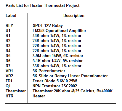
The circuit diagram shows the configuration of the HVAC thermostat. The LM358 Op Amp is used as a comparator to sense the inputs of the reference voltage (PIN 3) and room temperature (PIN 2). The thermistor used is a NTC (negative temperature coefficient) type where its resistance will drop when the temperature increases and vice versa. It has a resistance of 20K ohm at 25 degree Celcius. When the room temperature drops, the thermistor resistance will go up and hence the output of the operational amplifier will be low. This cause the relay to turn OFF and the heater will conduct until the temperature of the room rises again.


The circuit is calibrated using variable resistor VR1. Set the lever of the slide potentiometer or rotary potentiometer VR2 to 25 Celcius location. Place the thermistor at a space where the temperature is at 25 Celcius. By varying VR1, set the resistance at the position between the ON and OFF of the relay. Use a suitable contact relay rating according to the load of the heater.

Parts List


Read more...

DATA ACQUISITION SYSTEM

>> Saturday, April 17, 2010

Assembly
Please read all these instructions through once
before starting assembly. First note that 4
components are mounted underneath the double
sided, plated through PCB. The overlay shows these
components but they are mounted
UNDERNEATH the board on the copper side of
the PCB. The 4 components are C7 C8 R5 & R2.
C7, the 10uF tantalum capacitor must be pushed
over on its side so that the total height from the
surface of the PCB is under 5mm (otherwise it will
not fit inside the case.) The ceramic capacitor, C8,
also needs to be pushed over a little. The 1/8W
resistors will be under 5mm above the board.
All the other components are on the top of the PCB
as normal. Again the tantalum capacitor must be
pushed over to be under 5mm high. Make sure to
identify C6, the 103 monoblok capacitor and get it
in the right position. Make sure also that the two 10
pin IC’s are soldered in the right positions. U2 is the
MAX186. Note the orientation of the 1N4148
diode. The 78L05 must be mounted flush on the
PCB so it is not above 5mm. The resistor networks
can be either way around.
Make sure that the two DB25 connectors are
correct: J1 is male, J2 is female. Use one half of the case as a jig to hold the connectors & the PCB
before you solder any lugs. If you do not do this
then you run the risk that a connector will be skew
on the PCB & not fit properly into the case at both
ends.
The extra male DB25 connector & case are
provided for the power supply & inputs as
described in the documentation.
COMPONENTS KIT
0.1 104 monoblok .........C1 C2 C3 C5 .......... 4
0.01uF 103 monoblok ...C6 ........................... 1
1/8W 5% resistor
1K brown black red .....R5 ........................... 1
10K brown black orange R2 ......................... 1
10R brown black black .R1 ........................... 1
1N4148 diode ...............D1 ........................... 1
4.7uF/16V tantalum .......C4 ........................... 1
10uF/16V tantalum ........C7 ........................... 1
4K7 resistor network .....R3 R4 ...................... 2
74HCT373 ...................U1 ........................... 1
78L05 ...........................Q1 ........................... 1
220pF capacitor ............C8 ........................... 1
MAX186 ......................U2 ........................... 1
K118 PCB ..................................................... 1
D shell snap set ............................................... 1set
Male 25 pin PCB connector ......................... 2
Female 25 pin PCB connector ........................ 1
DB25 shell case .............................................. 1

FOR SOFTWARE VISIT www.electronickits.com/kit/complete/data/ck2000.htm

Read more...

5 BAND GRAPHIC EQUALIZER

This circuit uses a single chip, IC BA3812L for realizing a 5 band graphic equalizer for use in hi-fi audio systems.The BA3812L is a five-point graphic equalizer that has all the required functions integrated onto one IC. The IC is comprised of the five tone control circuits and input and output buffer amplifiers. The BA3812L features low distortion, low noise, and wide dynamic range, and is an ideal choice for Hi-Fi stereo applica-tions. It also has a wide operating voltage range (3.5V to 16V), which means that it can be adapted for use with most types of stereo equipment.

The five center frequencies are independently set using external capacitors, and as the output stage buffer amplifier and tone control section are independent circuits, fine control over a part of the frequency bandwidth is possible, By using two BA3812Ls, it is possible to construct a 10-point graphic equalizer. The amount of boost and cut can be set by external components.

The recommended power supply is 8V, but the circuit should work for a supply of 9V also. The maximum voltage limit is 16V.


The circuit given in the diagram operates around the five frequency bands:

  • 100Hz
  • 300Hz
  • 1kHz
  • 3kHz
  • 10kHz

Read more...

DIGITAL VOLUME CONTROLLER

This circuit could be used for replacing your manual volume control in a stereo amplifier. In this circuit, push-to-on switch S1 controls the forward (volume increase) operation of both channels while a similar switch S2 controls reverse (volume decrease) operation of both channels.

A readily available IC from Dallas semiconductor, DS1669 is used here.

FEATURES:

  • Replaces mechanical variable resistors
  • Electronic interface provided for digital as well as manual control
  • Wide differential input voltage range between 4.5 and 8 volts
  • Wiper position is maintained in the absence of power
  • Low-cost alternative to mechanical controls
  • Applications include volume, tone, contrast,brightness, and dimmer control

The circuit is extremely simple and compact requiring very few external components.

The power supply can vary from 4.5V to 8V.


Read more...

2 TRANSISTOR FM VOICE TRANSMITTER

Warning:

Take care with transmitter circuits. It is illegal in most countries to operate radio transmitters without a license. Although only low power this circuit may be tuned to operate over the range 87-108MHz with a range of 20 or 30 metres.

Notes:

I have used a pair of BC548 transistors in this circuit. Although not strictly RF transistors, they still give good results. I have used an ECM Mic insert from Maplin Electronics, order code FS43W. It is a two terminal ECM, but ordinary dynamic mic inserts can also be used, simply omit the front 10k resistor. The coil L1 was again from Maplin, part no. UF68Y and consists of 7 turns on a quarter inch plastic former with a tuning slug. The tuning slug is adjusted to tune the transmitter. Actual range on my prototype tuned from 70MHz to around 120MHz. The aerial is a few inches of wire. Lengths of wire greater than 2 feet may damp oscillations and not allow the circuit to work. Although RF circuits are best constructed on a PCB, you can get away with veroboard, keep all leads short, and break tracks at appropriate points.


One final point, don't hold the circuit in your hand and try to speak. Body capacitance is equivalent to a 200pF capacitor shunted to earth, damping all oscillations

Read more...

CONTROL ELECTRICAL APPLIANCES USING PC

Here is a circuit for using the printer port of a PC, for control application using software and some interface hardware. The interface circuit along with the given software can be used with the printer port of any PC for controlling up to eight equipment .
The interface circuit shown in the figure is drawn for only one device, being controlled by D0 bit at pin 2 of the 25-pin parallel port. Identical circuits for the remaining data bits D1 through D7 (available at pins 3 through 9) have to be similarly wired. The use of opto-coupler ensures complete isolation of the PC from the relay driver circuitry.
Lots of ways to control the hardware can be implemented using software. In C/C++ one can use the outportb(portno,value) function where portno is the parallel port address (usually 378hex for LPT1) and 'value' is the data that is to be sent to the port. For a value=0 all the outputs (D0-D7) are off. For value=1 D0 is ON, value=2 D1 is ON, value=4, D2 is ON and so on. eg. If value=29(decimal) = 00011101(binary) ->D0,D2,D3,D4 are ON and the rest are OFF.


FOR SOFTWARE VISIT www.electronic-circuits-diagrams.com

Read more...

LIGHT BARRIER DETECTOR


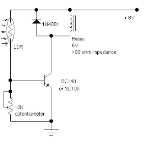
This simple circuit using a single transistor turns ON the relay when light falls on the LDR. The potentiometer is adjusted for the required sensitivity. The power supply is 6V. Be careful about the impedance of the relay. Its impedance should not be less that 60ohm. Its working can be explained as follows: With the light falling on the LDR,its resistance is low and the transistor is saturated and turns the relay ON. When light is obstructed, the LDRs resistance becomes very high. The potentiometer shorts the transistors base to ground and it is cut off. Hence the relay is OFF.

Read more...

OPTOCAL TOGGLE SWITCH

>> Friday, April 16, 2010

Using dual flip-flop IC CD4027 employ a 555 based monostable circuit to supply input clock pulses. The circuit described here obviates this requirement. One of the two flip-flops within IC CD4027 itself acts as square wave shaper


Read more...

TV REMOTE CONTROL BLOCKER

Just point this small device at the TV and the remote gets jammed . The circuit is self explanatory . 555 is wired as an astable multivibrator for a frequency of nearly 38 kHz. This is the frequency at which most of the modern TVs receive the IR beam . The transistor acts as a current source supplying roughly 25mA to the infra red LEDs. To increase the range of the circuit simply decrease the value of the 180 ohm resistor to not less than 100 ohm.

It is required to adjust the 10K potentiometer while pointing the device at your TV to block the IR rays from the remote. This can be done by trial and error until the remote no longer responds.


Read more...

500W LOW COST 12V TO 220V INVERTER

>> Thursday, April 15, 2010


Attention: This Circuit is using high voltage that is lethal. Please take appropriate precautions

Using this circuit you can convert the 12V dc in to the 220V Ac. In this circuit 4047 is use to generate the square wave of 50hz and amplify the current and then amplify the voltage by using the step transformer.


How to calculate transformer rating

The basic formula is P=VI and between input output of the transformer we have Power input = Power output
For example if we want a 220W output at 220V then we need 1A at the output. Then at the input we must have at least 18.3V at 12V because: 12V*18.3 = 220v*1
So you have to wind the step up transformer 12v to 220v but input winding must be capable to bear 20A.

Read more...

VGA TO TV SCART CIRCUIT

Description:

This is a circuit converter from VGA in TV SCART connection. Basically it is a circuit that accepts the signals from the exit of card VGA, him it then changes in combination RGB+composite sync and it leads to fastener SCART. The elements of picture from her exit card VGA, RED, BLUE and GREEN are already ready, bring right tendency the 0.the 7 vpp and right resistance of 75W for direct connection with fastener SCART, for depiction in the TV. What should it changes it is the right combination the horizontal and vertical synchronization signals from the VGA in a complex signal that will be led to the entry VIDEO in pin SCART. This transformation him they undertake electronic elements of circuit.

THAT IT FUNCTIONS

This circuit has been drawn in order to it changes regular signals VGA, standard RGB and the complex signal of timing. circuit is simple because signal RGB from the VGA is ready in standard level 0,7 Vpp and in 75W charge. For the signals of timing exists a circuit that changes the horizontal and vertical in complex. The circuit is simple based on a TTL completed with four gates XOR, two resistances and two capacitors. His choice completed TTL it is reasonable because the signals of timing of VGA they are signals TTL. The converter of signals of timing is system that regulates the difference of polarity of signals, so complex signal it is always right. Card VGA uses different polarities in the signals of timing in order to it informs the Monitor anymore analysis it uses. This circuit regulates the changes polarity the signals in least from 200 mSec, that are faster and from the time of regulation of common Monitor VGA. The circuit in order to function need stabilized tendency + 5V (+/- 5%) and current 120mA.

MANUFACTURE

Converter VGA in TV is easy in the manufacture to him it is enough exists a relative experience in the manufactures electronic. The circuit can be manufactured on one small EPOXY board. Remember only to connect also the completed circuit with the catering of 5V (in the drawing it does not appear). The circuit in order to it rightly functions it needs without fail stabilized tendency consequently it should you use also a REGULATOR LM7805. In the entry the 7805 the tendency should be from 9 until 16V so that it accomplishes us it gives the desirable stabilized tendency of 5V in his exit. Tendency from 9 until 16V we can him take also from our computer or from exterior small power supply's socket. From the computer we can we take from the following points: from door RS232, from the parallel door , from the PS2 and finally from a gambling chip of catering by his interior computer. Big attention should be given in him you stick that you will make and in the wiring of circuit, you avoid the chills you stick why the circuit functions in big frequency and sure will be created instabilities in the circuit with result bad quality of picture or even lack timing in the screen of TV. Be careful in order that the soldering is clean and glazing thus you will only be sure that the soldering has become right. For the wiring you are used shielded cables blentaz and ground the thorax of cables in the board's chassis. Good it is manufacture it is placed in a plastic box and it is placed and a connector EURO/scart female for placement in chassis.

MATERIALLY

U1: 74LS86
C1: 22mF
C2: 2,2 mF
R1, r2: 2k2
R3, r4, r5: 2k2
R6, r7, r9: 47k
R8: 120
T1, t2: 2N2222
Cable of connection VGA male 15pin sub D (DE 15)
Output connector 21pin EURO/scart female

VGA to TV Scart electronic circuit diagram

Read more...

2KM FM TRANSMITTER

Description.
With a matching antenna, the FM transmitter circuit shown here can transmit signals up to a range of 2 kilo meters. The transistor Q1 and Q2 forms a classic high sensitive preamplifier stage. The audio signal to be transmitted is coupled to the base of Q1 through capacitor C2. R1, R3, R4, R6, R5 and R9 are the biasing resistors for the preamplifier stage comprising of Q1 and Q2. Transistor Q3 performs the collective job of oscillator, mixer and final power amplifier.C9 and L1 forms the tank circuit which is essential for creating oscillations. Inductor L2 couples the FM signal to the antenna.

Circuit diagram.


Notes.
  • Assemble the circuit on a good quality PCB.
  • The circuit can be powered from anything between 9 to 24V DC.
  • Inductor L3 can be a VK220J type RFC.
  • For L1 make 3 turns of 1mm enamelled copper wire on a 10mm diameter plastic former. On the same core make 2 turns of 1 mm enamelled copper wire close to L3 and that will be L2.
  • Frequency can be adjusted by varying C9.
  • R9 can be used to adjust the gain.
  • For optimum performance, value of C8 must be also adjusted.
  • Using a battery for powering the circuit will reduce noise.

Read more...

STRAIN GAUGE

A strain gauge is a device that is used to measure the strain that occurs in an object. The device was invented in the year 1938 by Edward E. Simmons and Arthur Ruge. The device is still being used in many electronic circuits mainly as the principle sensing element for sensors like torque sensors, pressure sensors, load cells and so on.
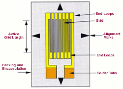
Strain Gauge working

Strain Gauge working

Strain Gauge Working Principle

Although strain gauges are available in many shapes and sizes, the fundamental working of this device is the same. They also vary in both shape and size according to their field of application.

A strain gauge consists of a foil of resistive characteristics, which is safely mounted on a backing material. When a known amount of stress in subjected on the resistive foil, the resistance of the foil changes accordingly. Thus, there is a relation between the change in the resistance and the strain applied. This relation is known by a quantity called gauge factor. The change in the resistance can be calculated with the help of a Wheatstone bridge.

TAKE A LOOK : WHEATSTONE BRIDGE

The strain gauge used is connected to the Wheatstone bridge with the help of an adhesive called cyanocrylate.

The property of the strain gauge not only depends on the electrical conductivity of the conductor, but also in the size and shape of the conductor used. As a matter of fact, the electrical conductivity also depends on the electrical conductance of the foil. This, in turn depends on the material of the conductor. The electrical resistance of the foil changes according to the change in the foil when it is stretched or compressed. The stretching or compressing is considered normal as long as there is no permanent change in the original appearance of the foil. Stretching causes an increase in the resistance from one end to other. Compressing causes a decrease in the resistance from one end of the conductor to another. Basically, the conductor will be a long strip with parallel lines with the condition that a little stress in the path of the orientation of the parallel lines will cause a resultant bigger strain multiplicatively over the effective length of the conductor. Thus a larger resistance change will be obtained.


The force applied to change elongate or shorten the strip can also be calculated with the help of the obtained output resistance.

An ideal strain gauge resistance varies from a few 3 ohms to 3 kilo ohms when it is unstressed. This value will change by a small fraction for the full force range of the gauge. It also depends on the elastic limits of the foil material. If there are forces applied to such an extent that they lose their original shape and size, the strain gauge will no longer be fit to use as a measuring device. So measurement of small fractional changes in the resistance must be taken accurately in order to use the strain gauge as a measuring device.

Applications

The voltage output in accordance to the stress is about a few millivolts. This voltage can be amplified to about 10 volts and can be applied to external data collection systems like recorders or PC data acquisition and analysis systems.

Strain gauges can be used to measure the stress developed in particular machinery and thus is used to mechanical engg. R&D.

The device is used aircraft component testing. Here also the measure of stress is the main issue. For this, strain gauges of very small size are connected to structural members, linkages and so on.

Gauge Factor Equation

The gauge factor of a strain gauge is given be the equation

GF = [∆R/RG]/E

∆R – Resistance produced by the strain

RG ­­– Resistance of gauge before application of stress

E – Strain produced

Types of Strain Gauges

This classification is based on the type of bridge circuit that is connected to the strain gauge. There are mainly three types of connections. They are

1. Quarter Bridge Strain Gauge Circuit

As shown in the diagram below, the imbalance is detected by the voltmeter in the center of the bridge circuit. The resistance R2 will be a rheostat and hence adjustable. The value of this resistance is made equal to the strain gauge resistance without the application of any force. The resistances R1 and R3 will have equal values. Thus, according to the Wheatstone bridge principle the entire circuit will be balanced and the net force will be zero. Thus the strain will also be zero. Now provide a compression or tension on the conductor and the circuit will be imbalanced. Thus you will get a reading at the voltmeter. Thus, the strain produced in response to the measured variable (mechanical force), is known as a quarter-bridge circuit.
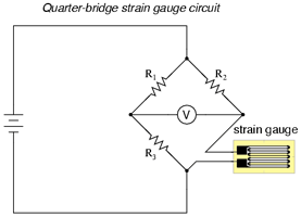
Quarter bridge strain circuit

Quarter bridge strain circuit

2. Half Bridge Strain Gauge Circuit

As shown in the circuit there are two strain gauges connected. If one of them does not respond to the strain produced it becomes a quarter bridge circuit. If both of them respond in such a way that both the strain gauges experience opposite forces it becomes a half bridge strain gauge circuit. By opposite forces, we mean that a compression on the upper strain gauge makes a stretch on the lower strain gauge. This causes both the gauges to make a better response to strain, thus increasing the response of the bridge to the applied force. As both the strain gauges act opposite and proportionally the response to the changes in temperature will be cancelled thus reducing the errors due to it.
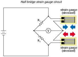
Half bridge strain gauge circuit

Half bridge strain gauge circuit

3. Full Bridge Strain Gauge Circuit

In the case of sensitivity, a half bridge strain circuit is more sensitive than a quarter bridge circuit. The sensitivity can be increased if all the elements of the bridge are active. Such a circuit is called full bridge strain gauge circuit. The circuit is also advantageous in the fact that it can be used to bond the complimentary pairs of strain gauges to the testing specimen. Thus, this is considered to be the best bridge circuit for strain measurement. The circuit is also advantageous because of its linearity. That is, the output voltage is exactly directly proportional to the applied force. But in the case of a half bridge and quarter bridge the output voltage is only approximately proportional to the applied force. Take a look at the circuit diagram given below.
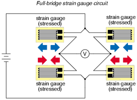
Full bridge strain gauge circuit

Full bridge strain gauge circuit

Read more...

FM ADAPTOR

Description.

With this compact FM adaptor circuit plugged into the audio out of your cassete player or i Pod out put,you can listen your favorite music on your car stereo.This circuit is very useful if your car stereo doesnot have an auxillary in socket.The circuit is nothing buy an short range FM transimitter.

The FM transmitter circuit is based on low power NPN transistor 2N2222.The tank circuit consisting of L1 & C1 producess the necessary oscillations at the collector of Q1.The capacitance C4 , resistance R3 & R4 performs the function of mixing the stereo out put from theaudio player or i-Pod.The emitter resistance R2 provides sufficient stability to the circuit.It also limits the collector current to increse the battery life.

Circuit diagram with Parts list.


Notes.

  • Use a 28SWG , 10 cm insulated copper wire as antenna.
  • For L1.make 8 turns of 20 SWG insulated copper wire on a 5mm dia plastic former.
  • Power the circuit from a 3V battery.
  • Assemble the circuit on a good quality PCB or common board.
  • C1 can be a 50pF trimmer.

Read more...

USB LAMP

>> Wednesday, April 14, 2010

>

Description.

Here is a simple USB powered lamp that can be used to light your desktop during power failures. The circuit operates from the 5 V available from the USB port.The 5V from the USB port is passed through current limiting resistor R2 and transistor Q1. The base of transistor Q1 is grounded via R1 which provides a constant bias voltage for Q1 together with D2.The diode D1 prevents the reverse flow of current from battery.C1 is used as a noise filter.Two white LED’s are used here for the lamp, you can also use a 2 V torch bulb instead of LED’s. LED D3 indicates connection with USB port.

Circuit Diagram with Parts List.

Read more...

USB SOUND CARD

Description.
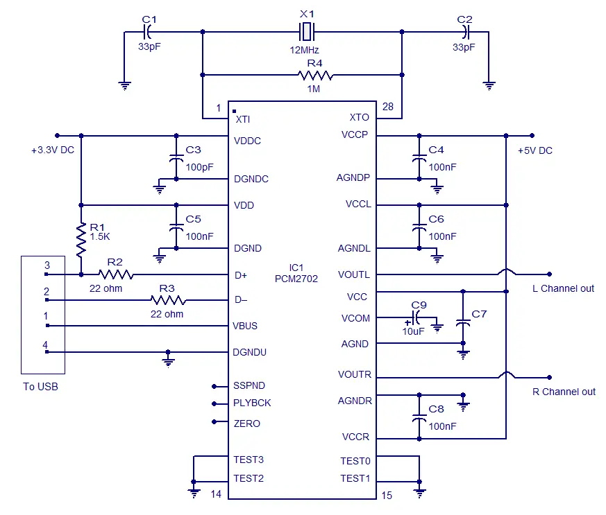
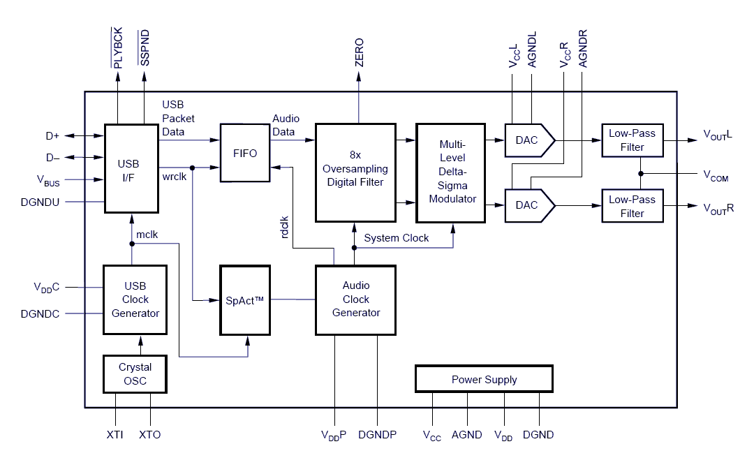
Designing and building a USB sound card is no longer a head ache because we have got the PCM 2702 integrated circuit from Texas Instruments. The PCM2702 is an integrated 16 bit digital to analog converter that has two digital to analog output channels. The integrated interface controller of PCM2702 is compliant to the USB 1.0 standards. The IC can handle sampling rates of 48 KHz, 44.1 KHz and 32 KHz. The IC also has a number of useful features like on-chip clock generator, digital attenuator, play back flag, suspend flag, zero flag, mute function etc. The most interesting thing is that this circuit is plug & play and doesn’t need any driver software for Windows XP and Windows Vista operating systems.

The circuit gets control data and audio data from the USB through the D+ and D- pins of the PCM2702 all the data transferring is carried out at full speed. The decoded audio signals will be available at the VOUTL and VOUTR pins of the IC. The 12MHz crystal is connected between the XT0 and XT1 pins of the IC. The VBUS (USB bus power) pin and DGND (digital ground) pins of the IC are connected to the +5V and ground pins of the USB respectively. The circuit requires +5V DC and +3.3V DC for operation and both of these voltages can be derived from the USB port using LDO (low drop out) voltage regulators (not shown in circuit).

Circuit diagram.

USB sound card

Block diagram of PCM2702.

PCM2702 block diagram

Notes.

  • +5V DC supply can be derived from the USB port using a +5V LDO regulator.
  • +3.3V DC supply can be derived from the USB port using a +3.3V LDO regulator.
  • Audio signals (output) available at VOUTL and VOUTR requires further amplification for driving low impedance head phones or loud speakers.
  • The PCM2702 is available only in SSOP28 package and requires special care while assembling.
  • Before attempting this circuit please go through the datasheet of PCM2702 and get a clear idea about the device.

Read more...

electronic keypad

Electronic Keypad electronic circuit diagram

Desctiption:

The IC is a quad 2 input "AND" gate, a CMOS 4081. These gates only produce a HIGH output, when BOTH the inputs are HIGH. When the key wired to 'E' is pressed, current through R1 and D1 switchs Q5 on.The relay energises; and Q5 is 'latched on' by R8. Thus, the Alarm is set by pressing a single key,say one of the two non-numeric symbols.

The alarm will switch off when the 4 keys connected to "A,B,C,D" are pushed in the right order.The circuit works because each gate 'Stands' upon its predecessor.If any key other than the correct key is pushed, then gate 1 is knocked out of the stack, and the code entry fails. Pin 1 is held high by R4. This 'Enables' gate 1; and when button 'A' is pressed, the output at pin 3 will go high. This output does two jobs.It locks itself 'ON' through R2 and it 'Enables' gate 2, by taking pin 5, high. Now, if 'B' is pressed, the output of gate 2, at pin 4 will go high. This output does two jobs. It locks itself 'ON' through R3 and it 'Enables' gate 3 by taking pin 12 high.

Now, if 'C' is pressed, the output of gate 3 will lock itself 'ON' through R5 and, by taking pin 8 high, 'Enable' gate 4. Pressing 'D' causes gate 4 to do the same thing; only this time its output, at pin 10, turns Q4 'ON'. This takes the base of Q5 to ground, switching it off and letting the relay drop out. This switches the alarm off.

Any keys not connected to 'A B C D E' are wired to the base of Q1. Whenever 'E' or one of these other keys is pressed, pin 1 is taken low and the circuit is reset. In addition, if 'C' or 'D' is pressed out of sequence, then Q2 or Q3 will take pin 1 low and the circuit will reset. Thus nothing happens until 'A' is pressed.Then if any key other than 'B' is pressed, the circuit will reset. Similarly, after 'B', if any key other than 'C' is pressed,the circuit will reset. The same reasoning also applies to 'D'. The Keypad needs to be the kind with a common terminal and a separate connection to each key. On a 12 key pad, look for 13 terminals. The matrix type with 7 terminals will NOT do. Wire the common to R1 and your chosen code to 'A B C D'. Wire 'E' to the key you want to use to switch the alarm on. All the rest go to the base of Q1.

The diagram should give you a rough guide to the layout of the components, if you are using a stripboard. The code you choose can include the non-numeric symbols.In fact, you do not have to use a numeric keypad at all,or you could make your own keypad. I haven't calculated the number of combinations of codes available, but it should be in excess of 10 000 with a 12 key pad; and, after all, any potential intruder will be ignorant of the circuit's limitations. Of Course, if you must have a more secure code, I can think of no reason why you shouldn't add another 4081 and continue the process of enabling subsequent gates. Or you could simply use a bigger keypad with more "WRONG" keys. Any small audio transistors should do. The 27k resistors could be replaced with values up to 100k. And the only requirements for the 4k7 resistors is that they protect the junctions while providing enough current to turn the transistors fully on. Capacitors (C1 C2 C3 C4 C5) are there to slow response time and overcome any contact bounce. They are probably unnecessary.

Read more...

single chip fm radio

Description.

Here is a compact low cost FM radio circuit using IC7400. This circuit is designed as per the data sheet and the result is excellent.Ideal for all category of electronic enthusiasts.

The TDA7000 is a monolithic integrated circuit for mono FM portable radios, where a minimum on peripheral components is crucial. The IC TDA 7000 has a Frequency-Locked-Loop system with an intermediate frequency of 70 kHz. The intermediate frequency selectivity is achieved by active RC filters. The only function which needs alignment is the resonant circuit for the oscillator, thus selecting the reception frequency. Spurious reception is avoided by means of a mute circuit, which also eliminates too noisy input signals. Special steps are taken to meet the radiation requirements.

Circuit Diagram with Parts List.


Notes

  • For L1 and L2 wind 5 turns of 0.6 mm enameled Copper wire on a 4 mm dia plastic former.
  • For antenna use a 50mm long insulated copper wire.
  • IC TDA 7000 can withstand up to 10 V supply voltage.But I recommend 6V.
  • Use an 8 Ohm speaker or Headphone at the audio output.

Read more...

ONE TRANSISTOR FM RECEIVER


This radio

is sensitive enough to tune 20 stations across the FM band, some with volume high enough to drive a small PM speaker. The ability to tune 88.9 MHz and 89.1 MHz is testimony of its selectivity. The signal-to noise ratio rivals that of the better walkman type radios.

Read more...

LONG DISTANCE VIDEO WIRE

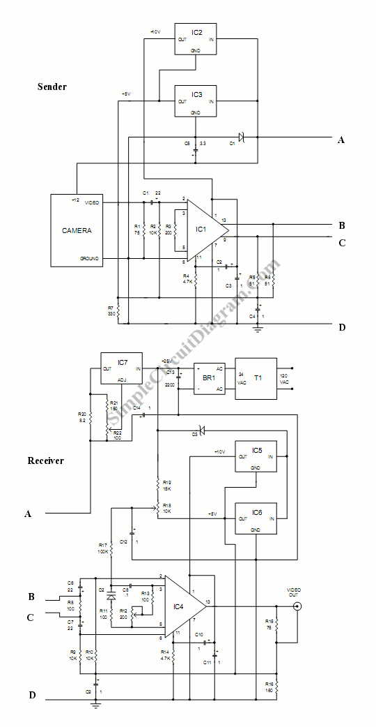
This circuit is used to connect the camera with very log wire. This is actually a video amplifiers. This circuit consist of two part, they are sender part and receiver part. At the sender part, this circuit uses an amplifier to make a stronger signal. So the signal can be transmitted through the long cables. To transmitted the signal, this circuit uses balanced mode, where two wires are driven in the opposite phase. Here is the schematic diagram :

video wire circuit circuit schematic diagram
The resistance of a typical four conductor flat 28 gauge telephone wire is about 7 ohms per 100 feet. Since voltage drops appear in both the plus and minus power supply leads, the total series resistance is about 14 ohms per 100 feet. Maximum allowable wire length depends on the total current requirements of the camera and send board. Using a camera that draws 100 ma, for example, a total current of about 180 ma is required and therefore a maximum of approximately 500 feet of 28 gauge flat telephone wire can be used. If a longer wire is needed, the round type of 22 gauge four conductor telephone wire offers much lower resistance. Its resistance per 100 feet is approximately 3.3 ohms total for both the positive and negative power wires. Using this wire and a 100 ma camera, the wire length can be approximately 2000 feet.

Parts:
* C1 – 22 mfd 6.3 volt tantalum
* C2, C3, C4, C9, C10, C11, C12 – 1 mfd 16 volt tantalum
* C5 – 3.3 mfd 16 volt tantalum
* C6, C7 – 22 mfd 16 volt tantalum
* C8 – .1 mfd 50 volt metalized film
* C13 – 2200 mfd 50 volt electrolytic
* C14 – 1 mfd 50 volt tantalum
* R1, R15 – 75 ohms 1/8 watt
* R2, R9, R10 – 10K 1/8 watt
* R3 – 200 ohms 1/8 watt
* R4, R14 – 4.7K 1/8 watt
* R5, R6 – 51 ohms 1/8 watt
* R7 – 330 ohms 1/8 watt
* R8, R11, R13 – 100 ohms 1/8 watt
* R12 – 200 ohms potentiometer
* R16 – 160 ohms 1/4 watt
* R17 – 100K 1/8 watt
* R18 – 10K potentiometer
* R19 – 15K 1/8 watt
* R20 – 8.2 ohm 1/2 watt
* R21 – 150 ohm 1/8 watt
* R22 – 100 ohm potentiometer
* R dummy – 100 ohm 2 watt
* D1 – 12 volt 1 watt zener diode
* D2 – Motorola MVAM109 tuning diode
* D3 – 10 volt 1 watt zener diode
* BR1 – 1 amp 400 volt DIP bridge rectifier
* IC1 – Maxim MAX435 dual output amplifier
* IC2, IC3, IC5, IC6 – 78L05 voltage regulator
* IC4 – Maxim MAX436 single output amplifier
* IC7 – LM317 adjustable voltage regulator
* J1 – RJ11 6P4C telephone jack with leads
* J2 – RJ11 6P4C board mount telephone jack
* J3 – chassis mount angle coaxial F connector
* T1 – 24 volt AC 400 ma adapter transformer
* eight 6-32 X 1/4 inch screws
* rubber grommet for 1/4 inch hole
* 2.2 X 3.3 X 4 inch metal enclosure with vent holes
* four conductor telephone wire with RJ11 plugs
* TO220 5 watt clip on heat sink
* four threaded spacers 6-32 X 1/2 inch long

The MAX435 transconductance amplifier is used as the core of this circuit. This circuit has wide bandwidth feature that is suitable for video signal application. To make sure that any noise exposing the cables would cancel each other at the receiver, this circuit uses balanced mode.

Read more...

water level controller

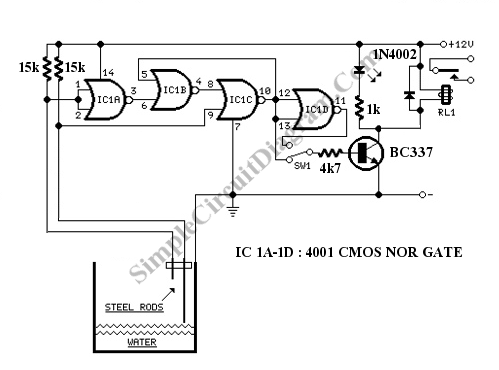
A controller for keeping the water level stays between upper and lower limits is described here. This water level controller is actually a water pump controller that turn the pump on or off based on the detected water level. This water level controller has two modes: fill and empty. Here is the schematic diagram of the circuit:

water pump controller circuit schematic diagram

For the empty mode, the water pump is used to suck the water from the tank. If the water reach the upper level limit, the pump will be turned on to drain the tank, until the level falls down to the lower level limit. At the fill mode, the pump is used to fill the tank with water, thus if the water level falls below the lower limit, then the pump will be turned on to fill the tank with the water. The SW1 set the mode, with the empty mode default value (as shown in the schematic).


Read more...

sound operated relay

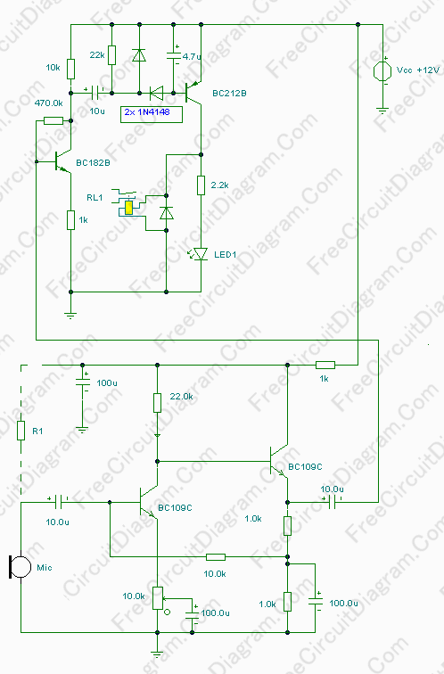
This circuit is not a voice operated switch (VOX) because this circuit is too dumb to differentiate between musical sound or human voice. This is rather a sound activated than voice activated. One interesting application is to control your disco lighting automatically by the musical sound from high power amplifier, when the music signal is dominating the sound space. The schematic diagram is shown below.

voice operated switch circuit schematic

You can use either moving coil microphone or condenser microphone for this circuit. For condenser microphone, you have to connect R1 resistor as shown by the dashed line. Choose between 1k5 ad 22k to adjust the sensitivity, or use a 4k7 value if you don’t care with the sensitivity fine tuning. Make sure the electrolytic capacitor is rated for 16 volt or more. The potentiometer shown in the schematic diagram is used to adjust the gain of the pre-amplification. You can adjust this potentiometer to get a proper sound level where the relay would be activated

Read more...

SIMPLE TEMPERATURE CONTROLLER

DESCRIPTION:
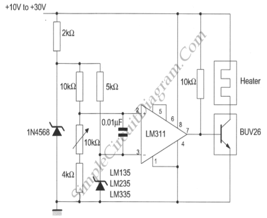
This temperature controller employs an LM135/235/335 temperature sensor, can be used to keep small environment warm or hot. Here is the schematic diagram:

Simple temperature controller

LM311 is used as comparator, to detect if the voltage at sensor pin (the inverting input) goes higher than the reference pin (the non-inverting pin). If this condition is detected, the comparator will switch off the heater driver (BUV26). Practically, after the desired temperature is met, the heater will be oscillating on-off, trying to keep the voltages at non-inverting input and inverting input equal

Read more...

positive to negative power supply by using simple 555 ic

DESCRIPTION:

If you need a negative supply for op-amp or just need negative bias voltage while operating from a single supply voltage (for battery operation for example), this circuit helps providing the negative supply for you. The circuit is based on charge pump driven by 555 switching circuit. Here is the schematic diagram:

negative supply 555 circuit schematic


The negative voltage produced by this circuit is about 1 volt smaller than the positive supply voltage magnitude. If you use 9V positive supply then the negative output will be around 8 volt, or if you use 12 volt positive supply the you’ll get around 11Volt negative supply. 100mA current could be drawn safely from the negative voltage output. This is enough for most op-amp or other small signal application.

Read more...

single tansistor FM

winding L1

L1 sets the frequency of the radio, acts as the antenna, and is the primary adjustment for super-regeneration. Although it has many important jobs, it is easy to construct. Get any cylindrical object that is just under 1/2 inch (13 mm) in diameter. I used a thick pencil from my son's grade school class, but a magic marker or large drill bit work just fine. #20 bare solid wire works the best, but any wire that holds its shape will do. Wind 6 turns tightly, side-by-side, on the cylinder, then slip the wire off. Spread the windings apart from each other so the whole coil is just under an inch (2.5 cm) long. Find the midpoint and solder a small wire for C2 there. Mount the ends of the wire on your circuit board keeping some clearance between the coil and the circuit board

Read more...

xmerless power supply

>> Tuesday, April 13, 2010

Description:

Here is a low cost and simple circuit that can be used to power up small electronics devices. The power is directly tapped from the mains via resistor R1.D1 rectifies the voltage and C1 and C2 are used to filter the output.The zener diode D2 keeps the voltage at steady 5V.


  • This circuit can deliver only up to 2omA ,there fore not suitable for serious circuits.
  • You can use this power supply for small LED circuits etc .
  • Remember you are playing with mains.Always be careful

Read more...

About This Blog

Lorem Ipsum

DISCLAIMER

I have not uploaded any contents on my own. I have got all these resources from the internet which are public and obtained as such from search engines. If these contents are objectionable or violating anyone copyrights please contact me. I will do the needful immediately and assure full assistance. No files are hosted on my server; they are only indexed much like how Google works. The hosting server or the administrator cannot be held responsible for the contents of any linked sites or any link contained in a linked site, or changes / updates to such sites. All stuff on this blog is for Entertainment and private Purposes only. It is not the purpose of this blog to infringe on anybody’s copyrights. Mail @ srikanth.tadhiparthi@gmail.com

  © Sunset by VINOD KUMAR 2008

Back to TOP